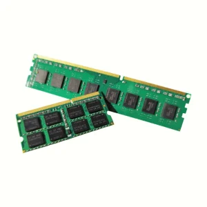
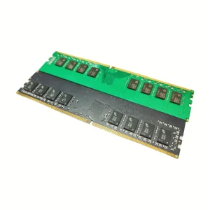
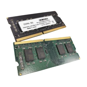
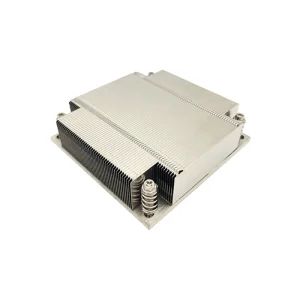
Direct supply of high-grade memory products, custom logic boards, and heat dissipators
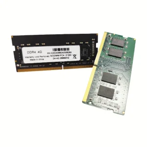
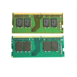
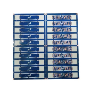
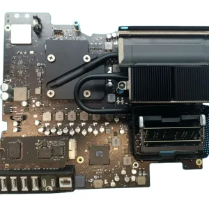
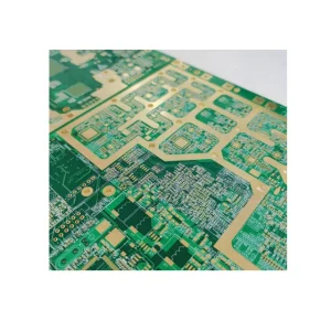
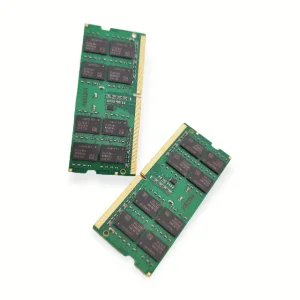
Double-sided printed circuit boards (PCBs) form the foundational layer of modern high-density electronics. Unlike single-sided options, double-sided variants allow routing on both surfaces, connected using Plating-Through-Hole (PTH) technology. This structural layout is essential for signal routing in server memory modules, enterprise storage systems, power distribution networks, and industrial computing assemblies.
Choosing the correct dielectric core material dictates impedance performance, thermal dissipation, and electrical loss characteristics. Depending on targeted frequencies and environments, we source and manufacture using several advanced substrates:
Advanced TDR testing ensures precise impedance matching within ±10% (standard) and down to ±5% for high-speed differential signal designs.
Options include ENIG (Electroless Nickel Immersion Gold), HASL Lead-Free, OSP, and Immersion Silver for optimal solderability and shelf life.
For double-sided PCB design stability, manufacturing tolerances must align with production capabilities. A mismatch leads to mechanical defects like copper peeling, solder bridging, and open circuits. We maintain tight parameters on line width, spacing, and registration:
Combining raw component supply with automated precision manufacturing ecosystems
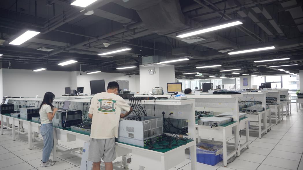
Operating out of our advanced electronic manufacturing facility in China, we leverage geographic supply chain clusters. In the electronics and PCB fabrication sector, latency of supply defines project velocity. With 14 years of industry experience, our teams bridge the gap between design layout optimization (DFM) and mass-production efficiency.
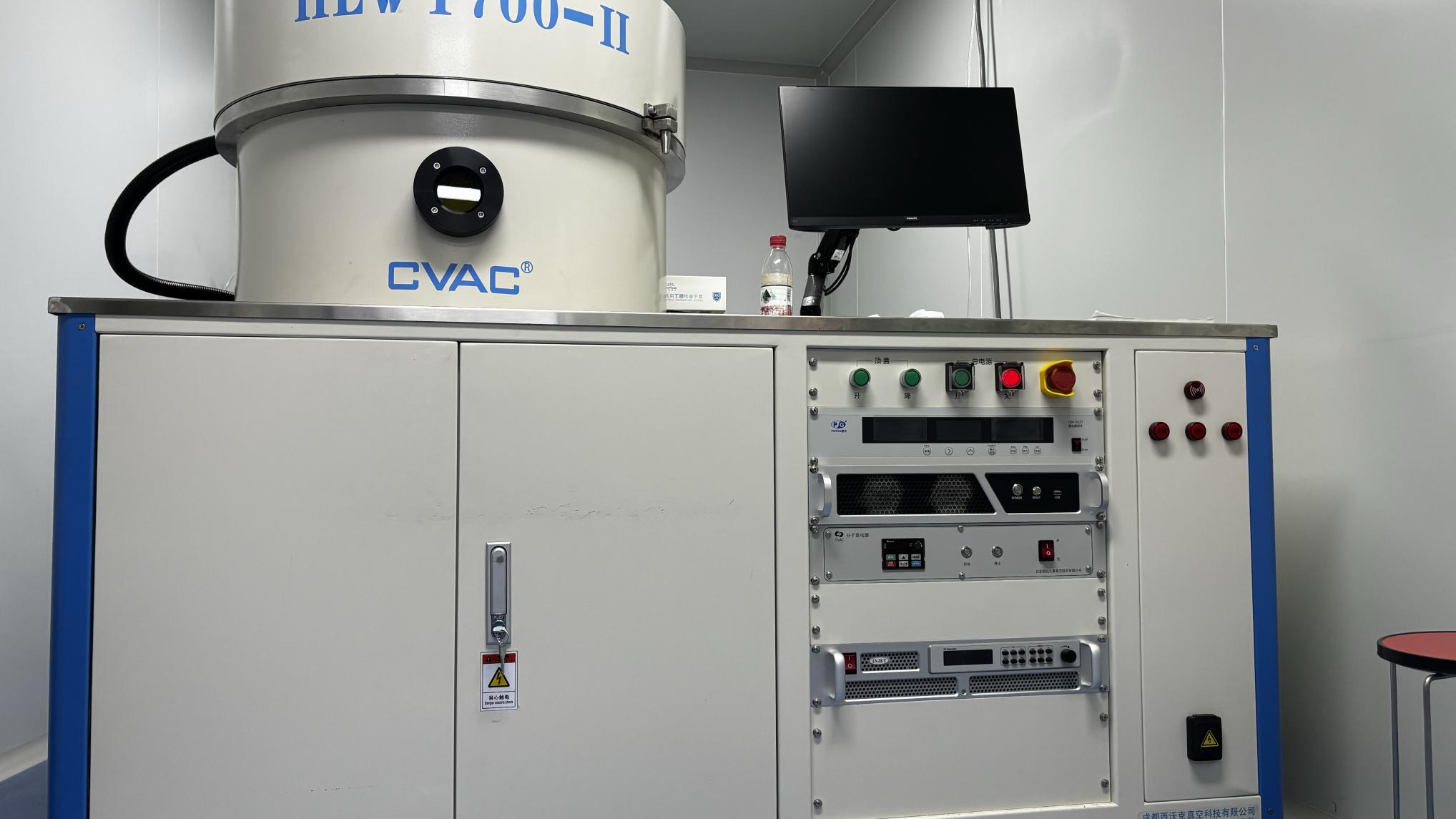
Our operation integrates automated optical inspection (AOI), high-precision drilling stations, automated electroplating lines, and flying probe testers. This structural consolidation enables us to provide comprehensive manufacturing solutions. Whether you require high-frequency multi-layer boards using Rogers substrates or high-volume double-sided circuit designs, our facility ensures rapid scaling, quality management, and international standards compliance.
Tailored engineering and board layout optimization across multiple electronic verticals
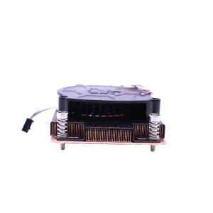
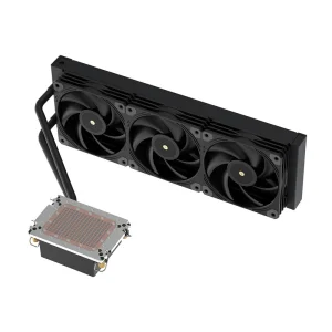
Providing high-frequency, low-loss mixed pressure PCBs with optimized thermal layouts. Tested for compatibility with high-power server memory slots and cooling blocks.
Our High-TG FR4 boards ensure reliable operations under continuous thermal loads, mechanical vibration, and power fluctuations inside automotive electronics.
Utilizing high-end PTFE and Rogers materials for 5G antenna units, low-noise amplifiers, and power distribution modules requiring strict dielectric tolerances.
Procuring custom printed circuit boards internationally requires stringent adherence to testing, quality standards, and environmental certifications. When sourcing from China, strategic buyers demand clarity on quality gates, DFM support, and logistics integration.
Every double-sided board and memory module leaving our facility undergoes rigorous verification:
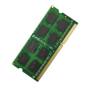
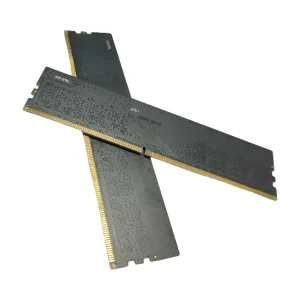
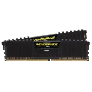
Your Trusted Global Partner for Advanced DDR5 Memory and Custom PCB Fabrication Solutions
Founded in 2017, Memvora Electronics Technology Co., Ltd. is a professional manufacturer specializing in high-performance DDR5 memory modules, dedicated to delivering reliable memory solutions for consumer, industrial, enterprise, and embedded applications worldwide. With a modern manufacturing facility covering 386㎡, we combine advanced production equipment, strict quality management, and experienced engineering expertise to provide stable, high-speed memory products for global OEM and ODM partners.
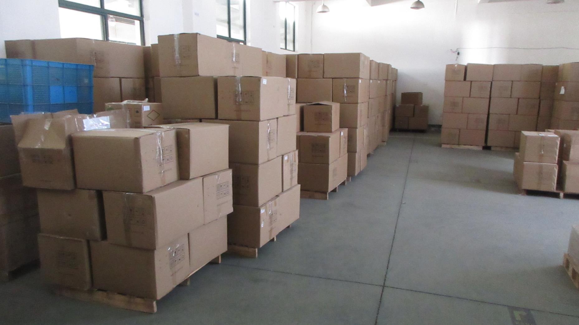
Since entering the international market, Memvora has accumulated 7 years of export experience, serving customers across North America, Europe, Southeast Asia, the Middle East, and South America. Our annual export revenue exceeds US$18.6 million, supported by a strong global supply chain and long-term partnerships with more than 1,280 component suppliers and business partners.
With 14 years of industry experience, our team continuously invests in technology innovation and product development. Our R&D department consists of 126 professional engineers who focus on developing next-generation DDR5 memory solutions with higher speed, lower latency, and enhanced reliability. Last year alone, we successfully launched 86 new memory products to meet the evolving needs of gaming, AI computing, industrial automation, and enterprise servers.
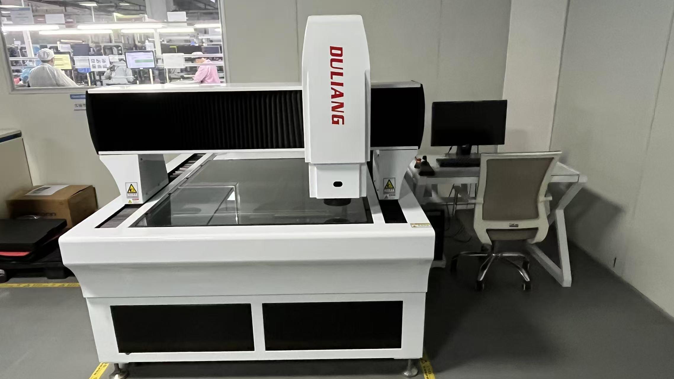
Quality is the foundation of everything we do. Every product undergoes 100% functional testing, burn-in testing, compatibility testing, signal integrity testing, and aging tests before shipment. Our dedicated quality control team of 42 inspectors ensures every memory module meets rigorous international quality standards and delivers long-term stable performance.
Memvora provides flexible OEM, ODM, private label, custom capacity, PCB color, heat spreader design, firmware optimization, and packaging customization services to meet different market requirements. Backed by a responsive engineering team and efficient production management, we help customers shorten development cycles and accelerate product launches.
Today, Memvora serves a diverse customer base including memory brands, computer manufacturers, industrial equipment suppliers, system integrators, distributors, wholesalers, and e-commerce retailers. Through continuous innovation, reliable quality, and customer-focused service, we are committed to becoming a trusted global partner for advanced DDR5 memory manufacturing and customized DRAM solutions.
Get professional answers regarding double-sided circuit board design, custom manufacturing, and logistics
Explore our high-performance board hardware, cooling mechanisms, and memory solutions