Frequently Asked Questions
What types of printed circuit boards can you manufacture?
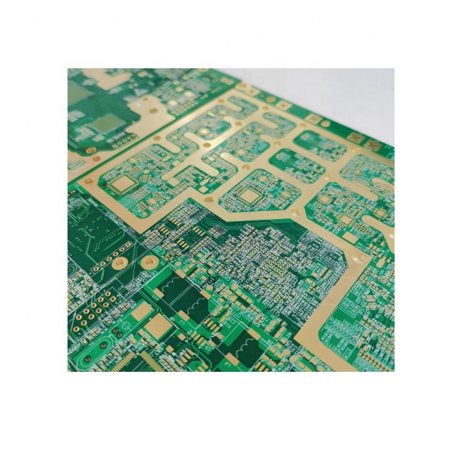
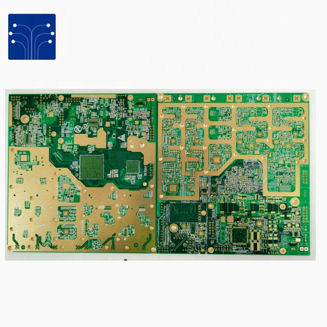
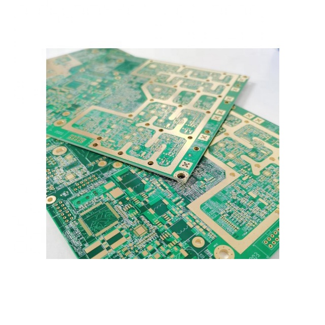
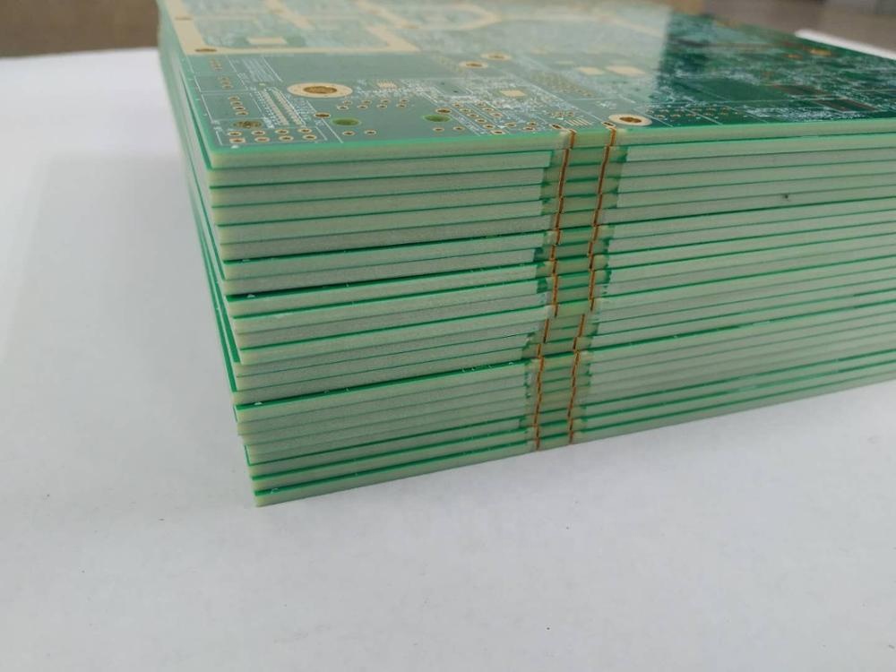
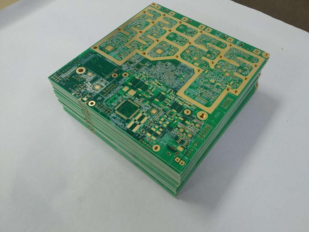
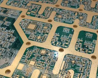
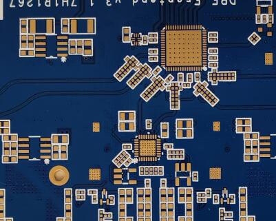
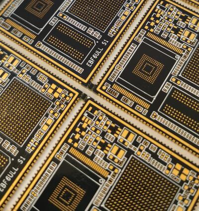
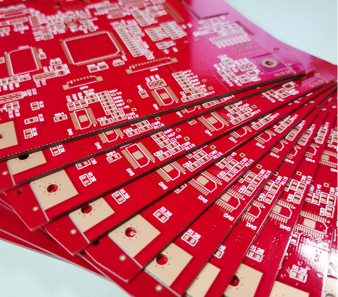
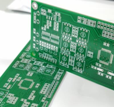
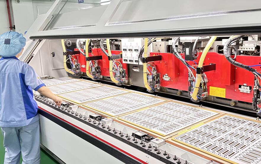
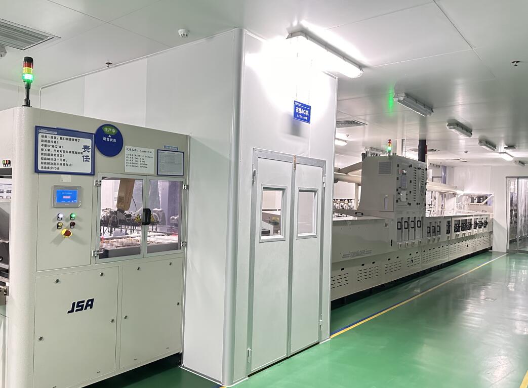
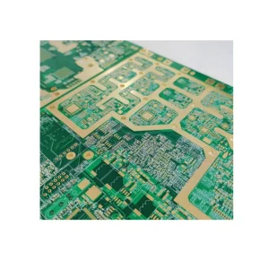
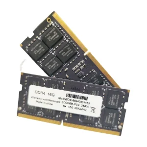
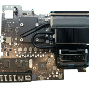
We specialize in manufacturing a comprehensive range of PCBs, including high-density multilayer boards (up to 68 layers), HDI, rigid-flex boards, impedance boards, high-frequency boards, high TG thick copper foil boards, 5G high-speed boards, buried blind via boards, and hybrid dielectric boards.
What is the fastest lead time for sample prototypes?
We provide expedited Quick Turn Around (QTA) services. Our shortest lead time for samples is 24 hours for 2-layer PCBs, 36 hours for 4-layer PCBs, and 48 hours for 6-layer PCBs. Standard lead times range from 3 to 10 days depending on layer count complexity.
What design file formats do your engineering teams accept?
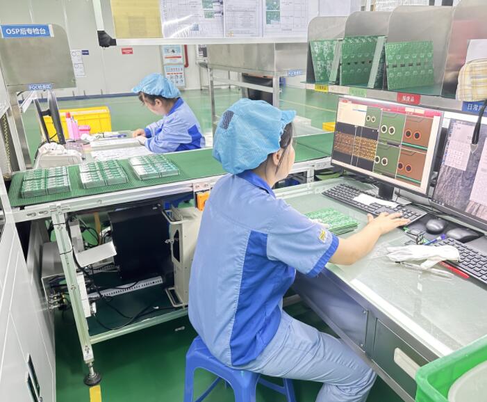
Our engineering division supports and accepts RS-274-X, RS-274-D CAD, DXP, Protel 99 SE, PADS, and GC-CAM file formats. Engineering reviews and queries are completed within 4 to 8 hours.
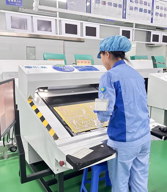
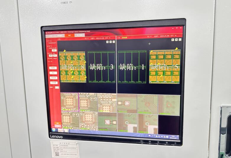
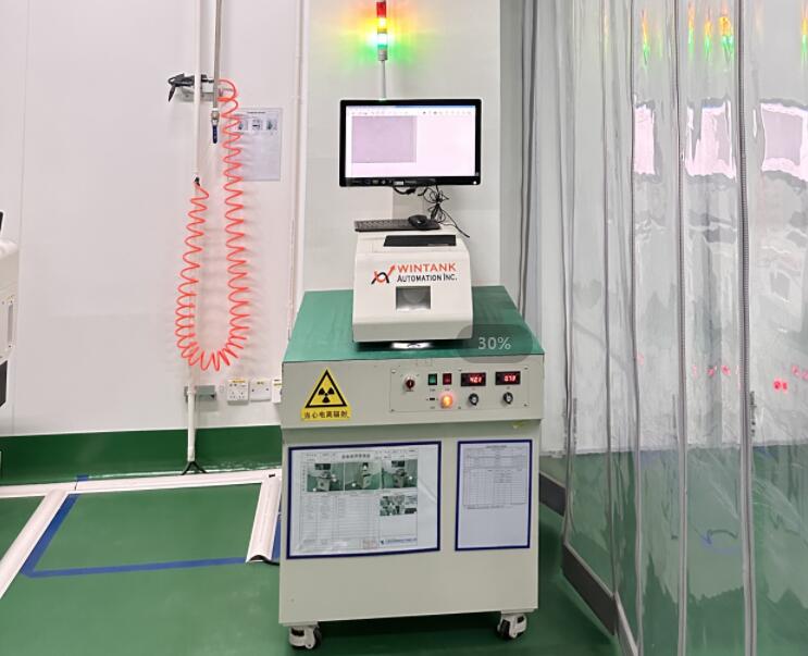
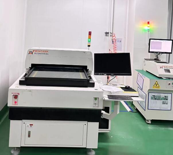
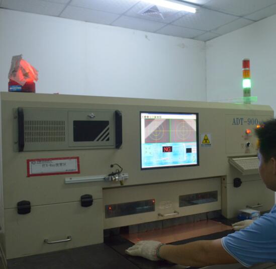
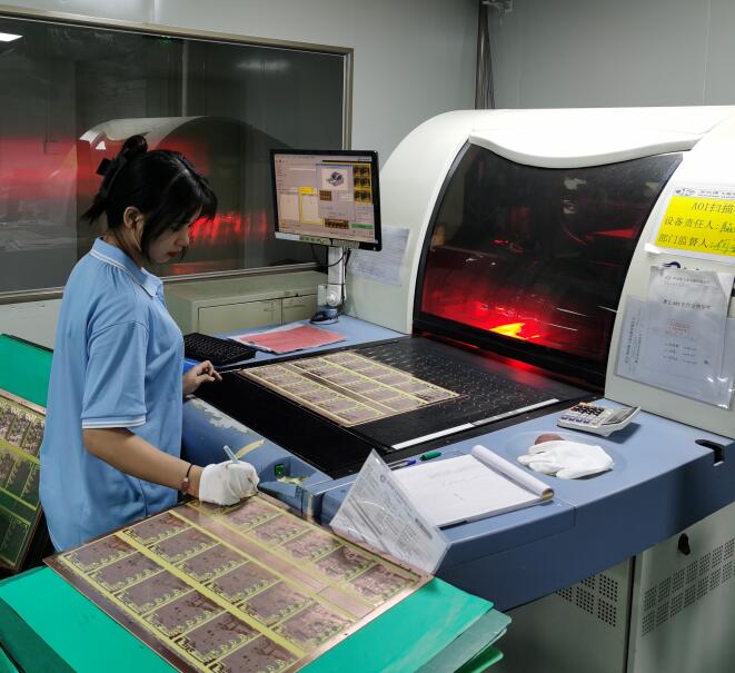
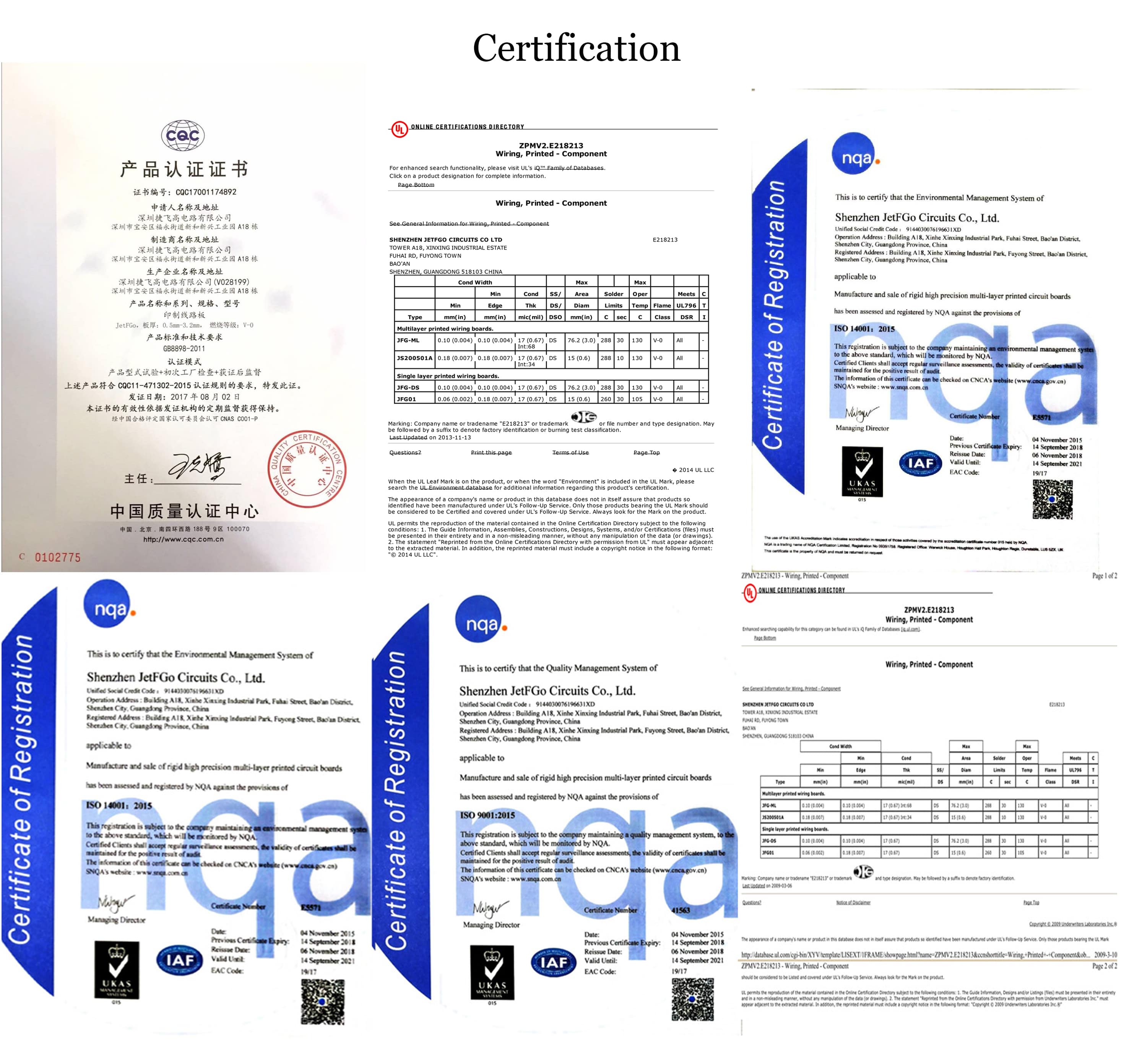
Which quality standards and certifications do you comply with?
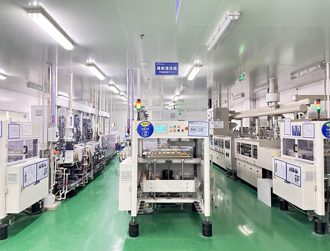
We strictly follow rigorous quality management standards and are certified in ISO 9001:2015, ISO 14001:2015, IATF 16949:2016, UL, CQC, RoHS, and REACH. All shipping and testing adhere to customer requirements and IPC standards.
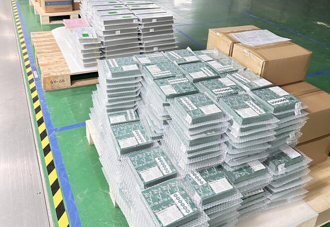
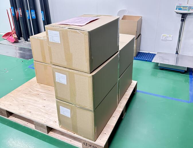
What shipping methods are available for orders?
We support multiple worldwide shipping options, including express air shipping via UPS, DHL, TNT, CTS, and FEDEX. We also offer railway cargo transit, ocean freight, or shipping using a customer's designated forwarder.
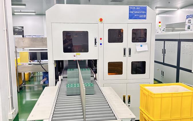
Do you support special PCB manufacturing techniques?
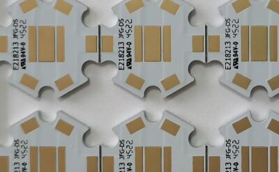
Yes, we support advanced techniques such as blind & buried vias, via in pad, semi-plated/castellated holes, counterbores, step mounting holes, mixed RF PCBs, and busbar PCBs. Custom volume specifications can be accommodated up to 30 oz max copper.