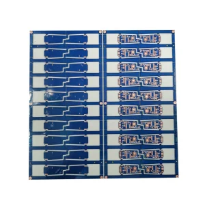
Mumbai, as the financial epicenter and industrial gateway of India, is experiencing an unprecedented surge in advanced electronics manufacturing. Under initiatives like "Make in India" and localized state policies, the Mumbai-Pune-Thane industrial corridor has transformed into a powerhouse for automotive electronics, power transmission systems, and IoT infrastructure. At the center of this technological leap is the Thick Copper Printed Circuit Board (PCB).
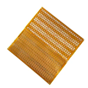
Thick copper PCBs (ranging from 3 oz/ft² to over 20 oz/ft² of copper thickness) are vital for handling high currents and managing extreme thermal dissipation. With Mumbai's booming electric vehicle (EV) automotive market, localized solar power grid storage projects, and heavy railway traction upgrades, global procurement teams are seeking reliable thick copper PCB suppliers who can combine localized delivery convenience with the engineering depth of global manufacturing facilities.
Historically, local manufacturing limitations in India restricted access to high-layer, high-density heavy copper solutions. Today, the collaboration between Mumbai-based engineering divisions and automated Chinese PCB fabrication plants has emerged as the most efficient model, offering complex multi-layer thick copper boards that feature optimal copper density distribution and high thermal conductivity.
As electric vehicles saturate the markets in Maharashtra, high-amperage components like traction inverters, battery management systems (BMS), and DC-to-DC converters rely heavily on thick copper traces to route currents of 200A and beyond without overheating.
Substation controls, switchgears, and heavy-duty transformers operating in humid coastal climates like Mumbai require heavy copper layers. Thick copper provides the mechanical stability and high-amperage capacity required to prevent catastrophic grid failures.
From motor drives to smelting controls, heavy industrial electronic applications require boards that resist vibration, handle high surge currents, and can be integrated directly with high-performance copper heat sinks.
For Mumbai-based industrial electronics OEM/ODM companies, sourcing thick copper PCBs involves striking a balance between strict quality standards (IPC Class 3 compliance) and economic viability. China's electronic manufacturing hubs offer a mature industrial ecosystem that local Indian alternatives cannot match in terms of scale and speed.
China-based plants utilize Vertical Continuous Plating (VCP) lines, which ensure uniform copper thickness across complex multi-layer boards. This technological edge prevents common heavy copper issues, such as uneven electroplating and excessive etching variations. Furthermore, raw materials like high-Tg FR-4 laminates (Tg170/Tg180) and oxygen-free high-conductivity copper foils are sourced directly from centralized material corridors, cutting down production lead times from weeks to days.
By coupling China's rapid prototype-to-volume manufacturing capabilities with Mumbai's local distribution channels, global procurement teams achieve a highly resilient and cost-optimized supply chain.
| Parameters | Standard Heavy Copper Specs | Advanced Capacity (Memvora Standard) |
|---|---|---|
| Copper Layer Thickness | 3 oz - 6 oz | Up to 20 oz (Customized options) |
| Laminate Types Available | FR-4, CEM-3 | High-Tg FR-4, Metal Clad, Polyimide, Halogen-Free |
| Thermal Conductivity | 1.0 - 2.0 W/m.K | Up to 4.0 W/m.K (Insulated Metal Substrates) |
| Min Line Width / Space | 0.15mm / 0.15mm | Optimized for heavy copper trace etching profiles |
| Surface Treatment | HASL, Lead-Free HASL | ENIG, Immersion Silver, OSP, Selective Plating |
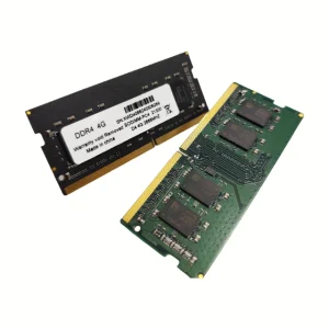
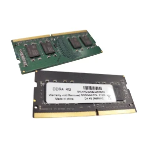
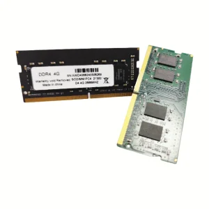
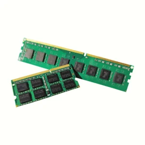
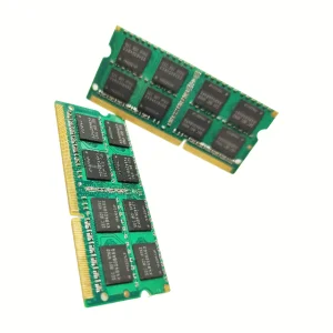
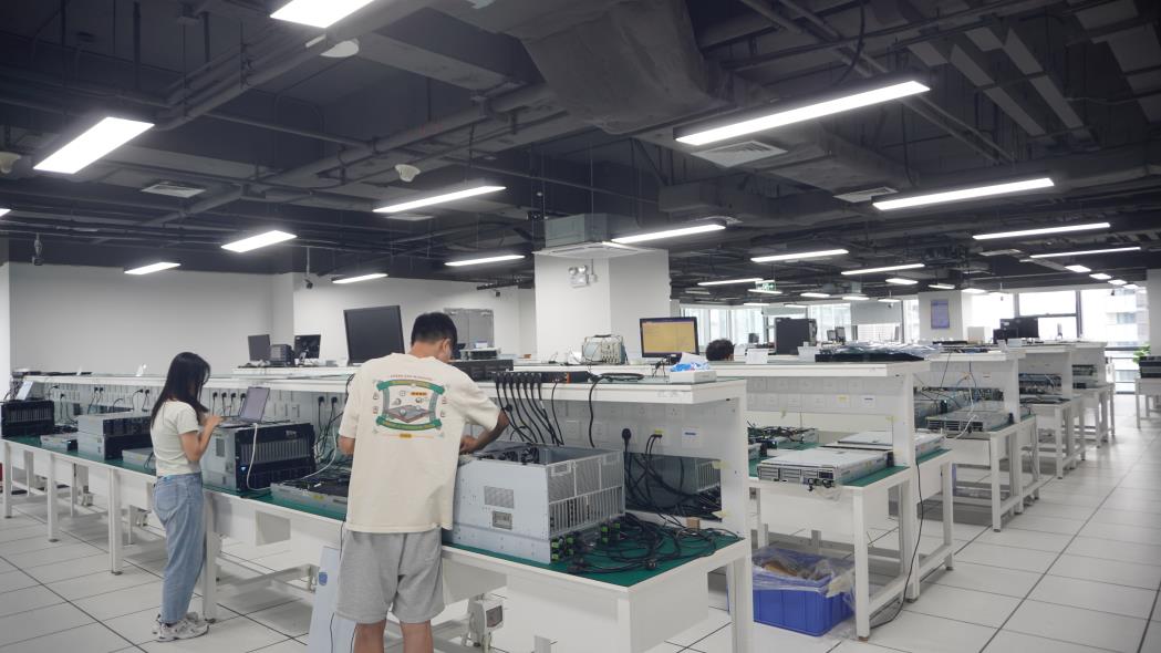
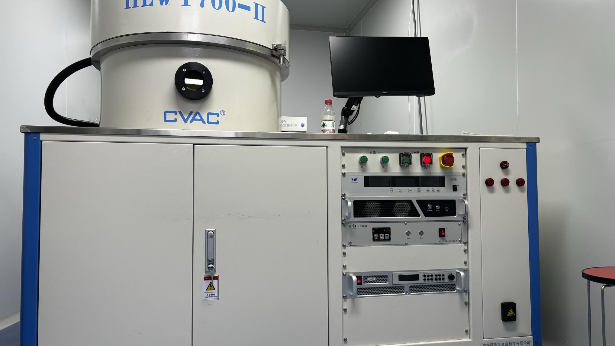
Founded in 2017, Memvora Electronics Technology Co., Ltd. is a professional manufacturer specializing in high-performance DDR5 memory modules and complex multi-layered system integration architectures, dedicated to delivering reliable memory and PCB-related solutions for consumer, industrial, enterprise, and embedded applications worldwide. With a modern manufacturing facility covering 386㎡, we combine advanced production equipment, strict quality management, and experienced engineering expertise to provide stable, high-speed products for global OEM and ODM partners.
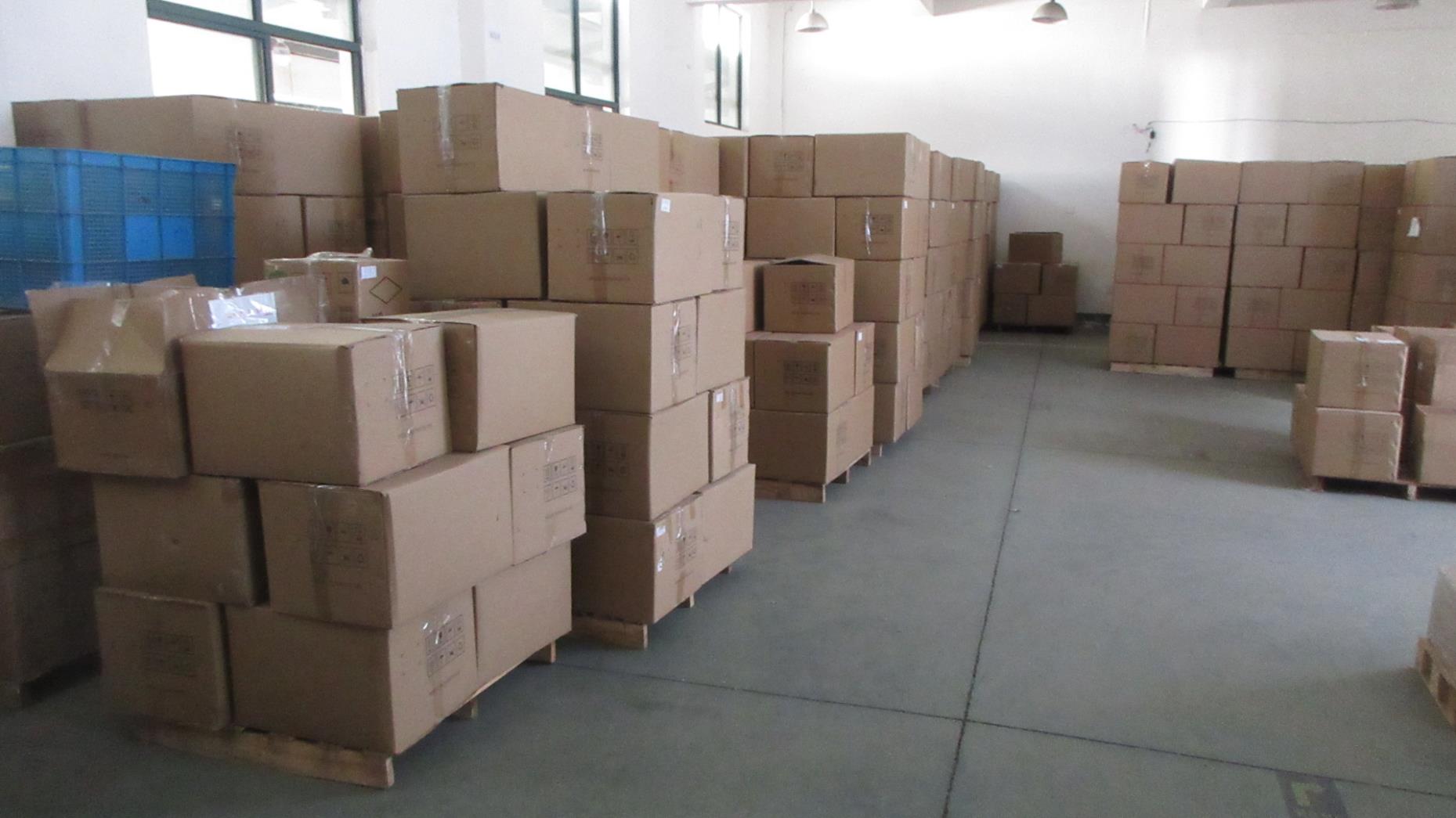
Since entering the international market, Memvora has accumulated 7 years of export experience, serving customers across North America, Europe, Southeast Asia, the Middle East, and South America. Our annual export revenue exceeds US$18.6 million, supported by a strong global supply chain and long-term partnerships with more than 1,280 component suppliers and business partners.
With 14 years of industry experience, our team continuously invests in technology innovation and product development. Our R&D department consists of 126 professional engineers who focus on developing next-generation memory and power integration solutions with higher speed, lower latency, and enhanced reliability. Last year alone, we successfully launched 86 new memory and computing products to meet the evolving needs of gaming, AI computing, industrial automation, and enterprise servers.
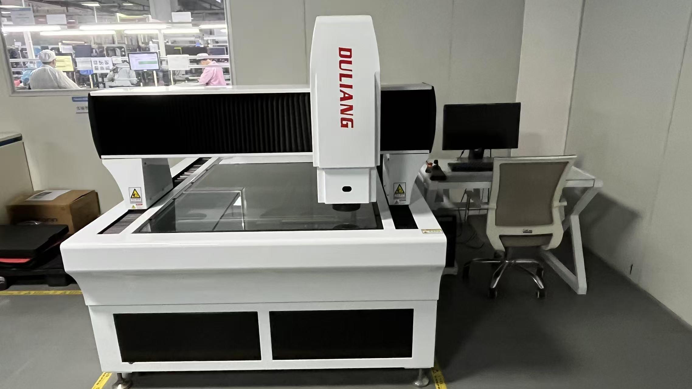
Quality is the foundation of everything we do. Every product undergoes 100% functional testing, burn-in testing, compatibility testing, signal integrity testing, and aging tests before shipment. Our dedicated quality control team of 42 inspectors ensures every module meets rigorous international quality standards (such as IPC and JEDEC) and delivers long-term stable performance.
Memvora provides flexible OEM, ODM, private label, custom capacity, PCB color, heat spreader design, firmware optimization, and packaging customization services to meet different market requirements. Backed by a responsive engineering team and efficient production management, we help customers shorten development cycles and accelerate product launches.
Designing a thick copper PCB for high-temperature zones like Mumbai requires precise trace dimension calculations. Following the IPC-2152 standards, trace width must match the target temperature rise (ΔT) and maximum current (Amperes) to prevent delamination.
For example, running a continuous current of 100A with a maximum allowable temperature rise of 20°C on a standard 3 oz copper layer requires a trace width of approximately 38mm (1.5 inches). However, by increasing the copper thickness to 6 oz, the required trace width drops to just 18mm, reducing the overall PCB footprint and allowing for tighter routing density.
To transfer heat away from high-power surface-mount components (like MOSFETs and IGBTs) to an external heat sink, a dense array of thermal vias must be designed. Memvora's fabrication facilities employ solid copper-plated vias to ensure low thermal resistance. Vias are filled with high-conductivity epoxy or copper pastes to maximize heat transfer efficiency, ensuring heat flows efficiently through the multi-layer stack-up.
Under heavy electrical loads, standard boards suffer from high thermal stress. We utilize high-Tg (glass transition temperature) laminates, typically Tg170 or Tg180, which maintain structural integrity and a low Coefficient of Thermal Expansion (CTE) even when undergoing continuous operating temperatures above 130°C.
This is particularly critical in hot and humid tropical climates like Mumbai, where ambient temperatures can fluctuate, exacerbating thermal stresses in industrial enclosures. Choosing the right material grade ensures the board will not delaminate during selective wave soldering or high-current operation.
Connect with Memvora's dedicated engineering support team to discuss your project guidelines, thermal rules, and custom multi-layer thick copper stack-ups.
Send Inquiry Now