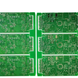
The electronics manufacturing services (EMS) ecosystem is undergoing a major paradigm shift. Hardware engineers, design houses, and enterprise procurement managers no longer view PCB Prototyping as a simple transactional service. In today's landscape, prototyping is the foundational crucible where hardware reliability, signal integrity, and cost-optimized mass manufacturability are established. As advanced technologies like 5G, artificial intelligence, automotive electrification (ADAS), and high-frequency edge computing expand, the margin for error in printed circuit board design has shrunk to zero.
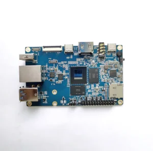
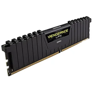
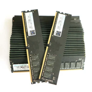
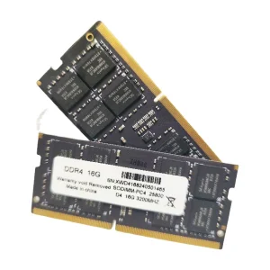
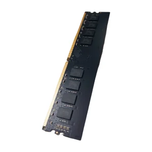
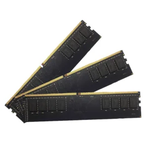
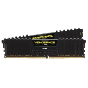
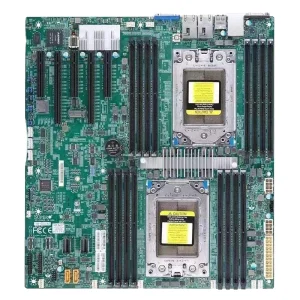
High-performance compute clusters, such as those hosting next-gen Rockchip RK3588S platforms, dual-channel server architectures, and dense DDR5 memory modules, demand multi-layer PCBs with strict impedance tolerances. Designing and fabricating these boards requires complex layer stacks, microvia control, and advanced surface finishes. Working with a prototyping manufacturer that bridges the gap between quick-turn fabrication and Design-for-Manufacturing (DFM) verification is critical to avoid costly mistakes and delayed product launches.
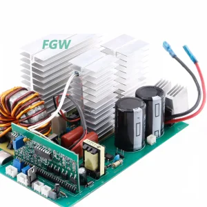
Modern electronic assemblies must operate under extreme thermal and electromagnetic conditions. Whether deploying high-power copper cooling blocks for LGA4189 processors, building rugged automotive power systems, or configuring multi-layer FR4/Rogers hybrid substrates, choosing the right PCB supplier determines the hardware's success. Industrial developers now require comprehensive lifecycle partnerships that include quick-turn prototyping, mass-scale component sourcing, and high-fidelity assembly.
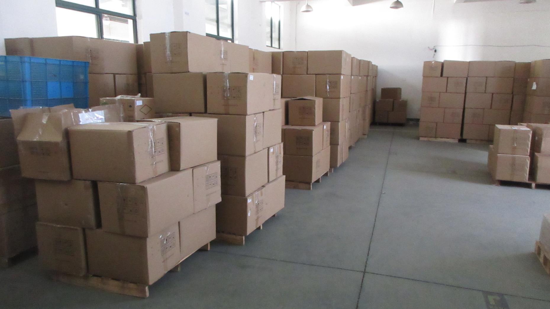
The hardware industry often relies on the phrase *“Shenzhen Speed”* to capture the efficiency of China's electronics manufacturing sector. This efficiency stems from a highly integrated supply chain that consolidates raw material refinement, component distribution, precision fabrication, automated SMT, and global logistics into one continuous process.
Raw substrates (FR-4, Rogers, Polyimide), advanced chemical copper plating, and components (ICs, passive chips, connectors) are sourced locally in real time. This eliminates transport delays and keeps materials close to the factory floor.
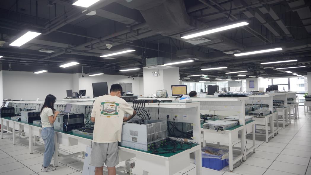
Equipped with state-of-the-art laser direct imaging (LDI), automated optical inspection (AOI), multi-axis drilling rigs, and high-speed pick-and-place lines, factories achieve consistency from prototype to volume production.
Combining high-speed surface mount technology (SMT) with precise dual-wave dual-chamber wave soldering for through-hole components (DIP) ensures strong mechanical connections and long-term electrical reliability.
Chinese manufacturers also help optimize the Bill of Materials (BOM). Local factories source direct replacements for passive components, connectors, and power chips. By using these pin-to-pin equivalents, hardware developers can maintain performance while reducing procurement costs and lead times. This allows businesses to transition from initial concept to high-volume production with minimal delays.
Different applications place distinct physical and electrical demands on PCB designs. Successful prototyping requires understanding these application-specific constraints early in the layout process.
| Application Field | Technical Challenges | Material & Design Options | Key PCBA Specifications |
|---|---|---|---|
| Enterprise Compute & Servers | Extreme signal speeds, high pin density, tight thermal limits, impedance matching. | High-TG multi-layer FR-4, Megtron 6, low-loss substrates. | 16+ layers, blind/buried vias, precise differential routing, ENIG. |
| Industrial Automation | Electrical noise, high operating currents, thermal cycling, environmental wear. | Thick copper traces (2oz-4oz), immersion silver, aluminum backing. | Wide spacing, conformal coatings, high-reliability DIP connections. |
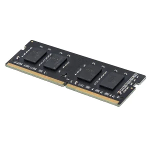
| Consumer Electronics & IoT | Compact footprints, thin profiles, battery space limits, cost control. | 1-2 layer flexible PCBs (FPC), ultra-thin FR-4 substrates. | 0201 component footprints, high-speed SMT assembly, selective gold plating. |
| Automotive Electronics (ADAS) | Vibration, extreme temperatures, zero-defect quality requirements. | Polyimide, specialized laminates, hybrid ceramic/FR-4 stackups. | IPC Class 3 compliance, 100% X-ray inspection, thermal vias. |
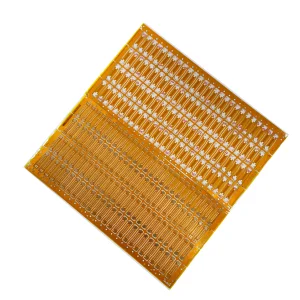
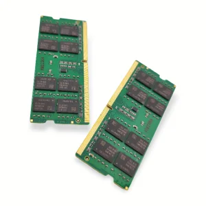
For instance, a flexible PCB (FPC) keyboard module requires dynamic flexibility, needing high-grade polyimide substrates that withstand millions of bending cycles. Conversely, a dual-channel server motherboard hosting DDR4 or DDR5 RAM requires high trace density, precise impedance matching, and dedicated ground planes to ensure clean data signals. Choosing the right material and manufacturing parameters early prevents signal reflections, EMI issues, and field failures.
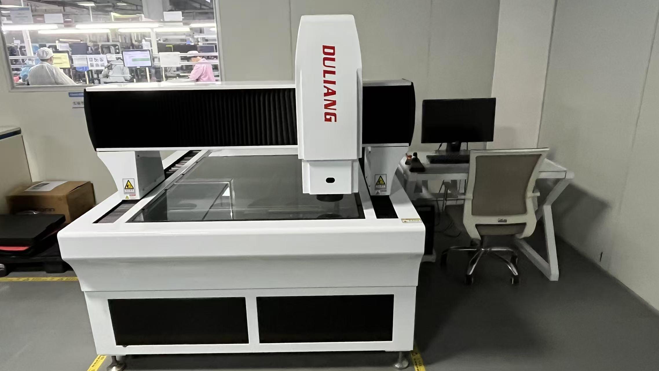
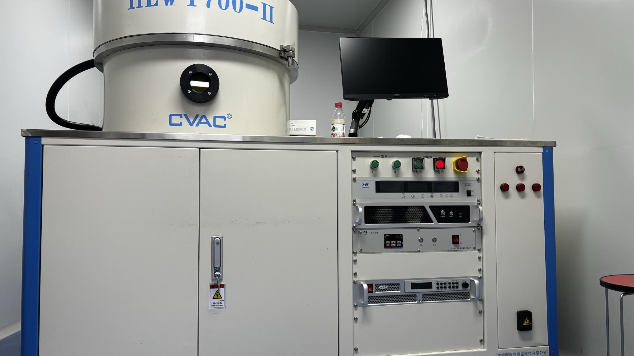
In the electronics industry, quality is defined by consistency, traceability, and yield. To evaluate the capabilities of a PCB manufacturer, procurement teams must look past basic marketing claims and focus on core technical standards:
By implementing these checks, procurement teams can reduce the total cost of ownership (TCO). Fast turnaround times for prototypes mean little if the resulting boards fail in assembly or in the field. Partnering with a supplier that integrates manufacturing expertise with robust quality controls ensures that prototypes scale to volume production smoothly.
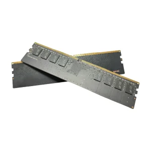
Founded in 2017, Memvora Electronics Technology Co., Ltd. is a professional manufacturer specializing in high-performance DDR5 memory modules, dedicated to delivering reliable memory solutions for consumer, industrial, enterprise, and embedded applications worldwide. With a modern manufacturing facility covering 386㎡, we combine advanced production equipment, strict quality management, and experienced engineering expertise to provide stable, high-speed memory products for global OEM and ODM partners.
Since entering the international market, Memvora has accumulated 7 years of export experience, serving customers across North America, Europe, Southeast Asia, the Middle East, and South America. Our annual export revenue exceeds US$18.6 million, supported by a strong global supply chain and long-term partnerships with more than 1,280 component suppliers and business partners.
With 14 years of industry experience, our team continuously invests in technology innovation and product development. Our R&D department consists of 126 professional engineers who focus on developing next-generation DDR5 memory solutions with higher speed, lower latency, and enhanced reliability. Last year alone, we successfully launched 86 new memory products to meet the evolving needs of gaming, AI computing, industrial automation, and enterprise servers.
Quality is the foundation of everything we do. Every product undergoes 100% functional testing, burn-in testing, compatibility testing, signal integrity testing, and aging tests before shipment. Our dedicated quality control team of 42 inspectors ensures every memory module meets rigorous international quality standards and delivers long-term stable performance.
Memvora provides flexible OEM, ODM, private label, custom capacity, PCB color, heat spreader design, firmware optimization, and packaging customization services to meet different market requirements. Backed by a responsive engineering team and efficient production management, we help customers shorten development cycles and accelerate product launches.
Today, Memvora serves a diverse customer base including memory brands, computer manufacturers, industrial equipment suppliers, system integrators, distributors, wholesalers, and e-commerce retailers. Through continuous innovation, reliable quality, and customer-focused service, we are committed to becoming a trusted global partner for advanced DDR5 memory manufacturing and customized DRAM solutions.